How to deal with Solder Mask Thickness Deviation on PCBAuthor : Adrian September 10,solder paste vs flux 2025Table of ContentsIf you're facing solder mask thickness deviation on your printed circuit board (PCB), you're not alone. This common issue can lead to uneven protection of copper traces, potential short circuits, and assembly problems. The good news? It can be managed with the right approach. In this comprehensive guide, we'll explore what solder mask thickness deviation is, why it happens, and how to address it effectively to ensure your PCB performs reliably.
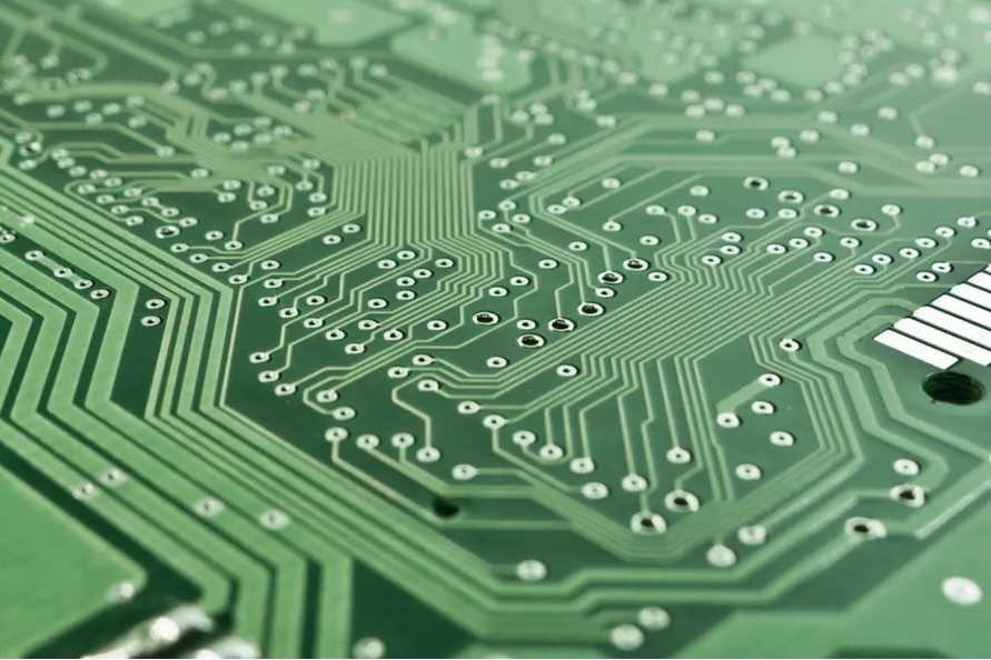
What Is a PCB and Why Does Solder Mask Matter?Before diving into the specifics of solder mask thickness, let's clarify what a PCB is. A printed circuit board is the backbone of electronic devices, providing a platform to connect and support electronic components like resistors, capacitors, and chips. It consists of layers of insulating material with conductive copper traces that form the electrical pathways. The solder mask is a thin protective layer, often green in color (though other colors like blue, red, or black are also used), applied over the copper traces on a PCB. Its primary role is to shield the copper from oxidation, prevent solder bridges during assembly, and protect against environmental damage like moisture or dust. When the solder mask thickness deviates—meaning it's uneven or not within the specified range—it can compromise these protective functions, leading to performance issues or even board failure.
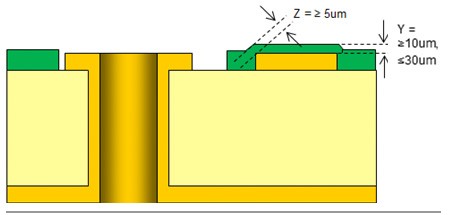
Understanding Solder Mask Thickness and Its ImportanceSolder mask thickness refers to the depth of the protective coating applied to the PCB. Typically, the standard thickness ranges from 0.8 to 1.2 mils (20 to 30 micrometers) on the copper traces and slightly thinner over the board's surface. Maintaining consistent thickness is crucial because:
When thickness deviates—either too thick or too thin—it can cause problems. For instance, a mask that's too thin may not protect the copper adequately, leading to oxidation. Conversely, a mask that's too thick might interfere with component placement or soldering precision.
Common Evenness Problems with PCB Solder MaskEvenness problems with PCB solder mask occur when the layer isn't applied uniformly across the board. This can manifest in several ways:
These issues not only affect the board's appearance but also its functionality. For example, exposed copper can oxidize, increasing electrical resistance and potentially causing signal integrity issues, especially in high-frequency applications where impedance control is critical (e.g., maintaining 50 ohms for RF signals).
Causes of Solder Mask Thickness DeviationUnderstanding why solder mask thickness deviation happens is the first step to addressing it. Several factors during the manufacturing process can contribute to this issue: 1. Inconsistent Application MethodsThe solder mask is typically applied using methods like screen printing, curtain coating, or spray coating. If the equipment isn't calibrated correctly or the process parameters (like pressure or speed) aren't controlled, the thickness can vary across the board. 2. Material Quality IssuesThe solder mask material itself—usually a liquid photoimageable polymer—must be of high quality. If the material has inconsistencies, such as varying viscosity, it can lead to uneven application. For instance, a viscosity outside the recommended range of 150-200 centipoise can cause flow issues during coating. 3. Improper Curing ConditionsAfter application, the solder mask is cured using heat or UV light to harden it. If the curing temperature (typically 120-150°C) or exposure time isn't uniform, some areas may not set properly, leading to thickness variations or adhesion problems. 4. Surface ContaminationBefore applying the solder mask, the PCB surface must be clean. Dust, oil, or residue on the board can prevent the mask from adhering evenly, resulting in thin spots or voids. 5. Design and Layout ChallengesThe PCB design itself can contribute to thickness deviation. For example, densely packed traces or varying copper heights (due to different trace widths, often ranging from 4 to 10 mils) can cause uneven mask distribution during application.
How to Identify Solder Mask Thickness DeviationDetecting solder mask thickness issues early can save time and cost during PCB production. Here are some practical ways to identify deviations:
Solutions to Address Solder Mask Thickness DeviationNow that we've covered the causes and identification methods, let's focus on actionable solutions to deal with solder mask thickness deviation on PCBs. These strategies span design, manufacturing, and quality control stages. 1. Optimize PCB Design for Uniform ApplicationStart by designing your PCB with solder mask application in mind. Ensure that trace heights and densities are as uniform as possible to avoid uneven coating. For instance, maintain consistent trace widths (e.g., 6 mils for standard designs) and avoid abrupt changes in copper density. Additionally, include clear solder mask clearance specifications in your design files—typically 2-4 mils around pads—to prevent overlap or insufficient coverage. 2. Choose the Right Solder Mask MaterialSelect a high-quality solder mask material suited for your application. Liquid photoimageable solder masks are common for their precision, but ensure the viscosity and curing requirements match your manufacturing setup. Work with your manufacturer to verify material consistency before production begins. 3. Calibrate Application EquipmentEnsure that the equipment used for applying the solder mask—whether screen printing or spray coating—is properly calibrated. Regularly check parameters like roller pressure, nozzle speed, and material flow rate to maintain uniform application. For example, in screen printing, a mesh count of 100-120 threads per inch often provides consistent results for standard PCBs. 4. Control Curing ConditionsMonitor the curing process closely. Maintain a consistent temperature (e.g., 130°C for thermal curing) and exposure time across the entire board. If using UV curing, ensure the light intensity is uniform to avoid under-cured or over-cured areas that could affect thickness or adhesion. 5. Implement Strict Surface PreparationClean the PCB surface thoroughly before applying the solder mask. Use chemical cleaning agents or micro-etching to remove contaminants like oil or oxide layers. A clean surface ensures better adhesion and even distribution of the mask material. 6. Conduct Regular Quality ChecksIntegrate quality control steps during and after production. Perform visual and microscopic inspections to catch thickness deviations early. Use automated optical inspection (AOI) systems if possible, as they can detect inconsistencies with high accuracy, often identifying defects smaller than 1 mil. 7. Collaborate with Your ManufacturerWork closely with your PCB fabrication partner to address thickness deviation issues. Share detailed design files and specifications, and request feedback on potential manufacturing challenges. Many deviations can be minimized by aligning design intent with production capabilities.
Preventing Future Solder Mask Thickness IssuesPrevention is always better than correction. Here are some long-term strategies to minimize solder mask thickness deviation in future PCB projects:
The Impact of Solder Mask Thickness on PCB PerformanceIt's worth emphasizing how critical solder mask thickness is to overall PCB performance. For high-speed designs, an uneven solder mask can alter the dielectric constant, affecting signal propagation speeds (often measured in picoseconds per inch). In power electronics, inadequate protection from a thin mask can lead to arcing or breakdown under high voltages (e.g., above 500V). By addressing thickness deviations, you ensure not just reliability but also compliance with industry standards like IPC-A-600, which specifies acceptable solder mask coverage and thickness tolerances.
ConclusionDealing with solder mask thickness deviation on PCBs doesn't have to be a daunting task. By understanding what causes unevenness, identifying issues early through inspection, and applying targeted solutions like optimized design and controlled manufacturing processes, you can achieve a uniform and reliable solder mask layer. Consistent thickness—typically 0.8 to 1.2 mils—ensures your PCB is protected, functional, and ready for assembly. Whether you're an engineer designing intricate boards or a manufacturer aiming for flawless production, addressing solder mask evenness problems is key to delivering high-quality electronics. With the tips and strategies outlined in this guide, you're well-equipped to tackle this common challenge and enhance the durability and performance of your PCBs. Share · · · · The Role of Flux in PCB Wave Soldering: Selection, Application, and Residue RemovalMarch 16, 2026PCB wave soldering flux types include rosin, water-soluble, and no-clean options with varying activity levels for oxide removal and solder flow. This guide covers selection criteria, spray foam drop-jet application methods, residue removal processes, and alternatives like nitrogen blanketing to boost joint reliability and yields for engineers. Article Achieving Uniform Solder Fillets in PCB Wave Soldering: Process ControlMarch 16, 2026Achieve uniform solder fillets in PCB wave soldering with process control strategies. Optimize flux, preheat, wave height, conveyor speed for consistent fillet shape, height, and wetting balance. Includes visual inspection tips and troubleshooting for reliable through-hole assemblies. Boost quality in production. Article Optimizing Conveyor Speed for Efficient PCB Wave SolderingMarch 16, 2026Learn PCB wave soldering conveyor speed calculation to manage dwell time, immersion depth, and throughput effectively. Electric engineers get practical steps, best practices, and troubleshooting tips for higher process efficiency and fewer defects in wave soldering operations. Article Understanding IPC Standards for PCB Surface Finishes: Ensuring Quality and ComplianceMarch 11, 2026Understand IPC standards IPC 4552 ENIG and IPC 4553 immersion silver for PCB surface finishes. Ensure compliance, enhance solderability, and prevent common defects to achieve reliable, high quality circuit boards. Article Miniaturization Challenges in PCB AssemblyMarch 11, 2026Navigate the complexities of high density interconnect PCB assembly and precise component placement. Learn to tackle miniaturization challenges, from tiny part handling to thermal stress, ensuring robust and reliable electronics. Article High Speed Routing Techniques: PCBMarch 11, 2026Master high speed routing in PCBs to ensure signal integrity and minimize electromagnetic interference. Learn essential techniques for robust designs, from controlled impedance to differential pair strategies. Prevent performance issues and achieve reliable electronics. ArticleGet Instant PCB |